
이메일 형식 오류
emailCannotEmpty
emailDoesExist
pwdLetterLimtTip
inconsistentPwd
pwdLetterLimtTip
inconsistentPwd


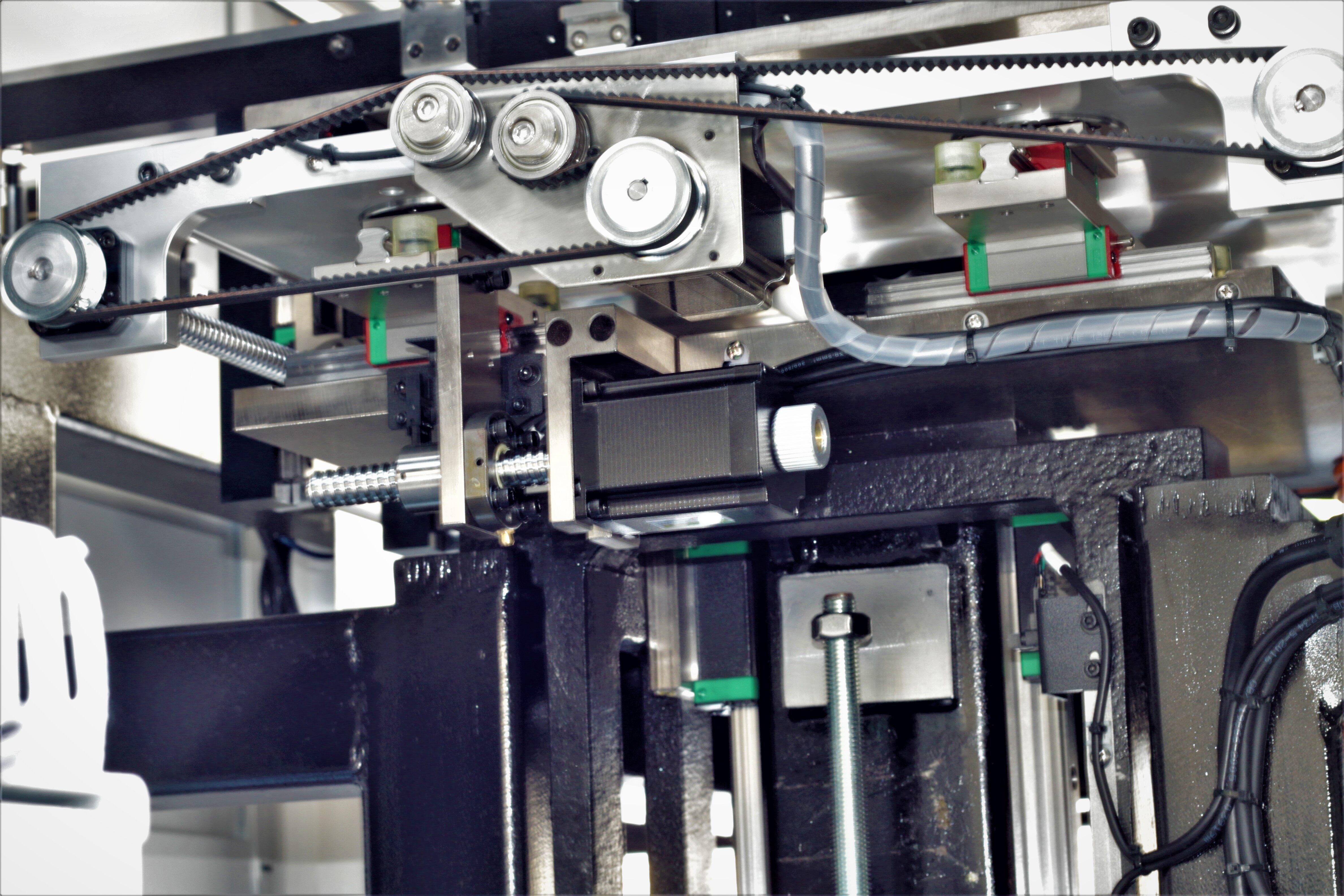
China Wholesale Selective Wave Soldering
Selective wave soldering is a specialized soldering process used in electronics manufacturing, primarily for through-hole components on printed circuit boards (PCBs). It's a variation of the traditional wave soldering process, but it's more precise and targeted, allowing for specific areas of the PCB to be soldered while leaving others unsoldered.
How the selective wave soldering process typically works:
-
Masking: Before the selective soldering process begins, areas of the PCB that don't require soldering are usually masked off. This can be done using various methods, such as applying a temporary solder mask or using masking tapes.
-
Preheating: The PCB is preheated to a specific temperature to prepare it for soldering. Preheating helps to activate fluxes and minimize thermal shock to components during the soldering process.
-
Selective Soldering: The PCB is then moved into position beneath a nozzle or a small solder wave. Unlike traditional wave soldering, where the entire PCB is passed over a wave of molten solder, in selective wave soldering, only specific areas of the PCB are exposed to solder.
-
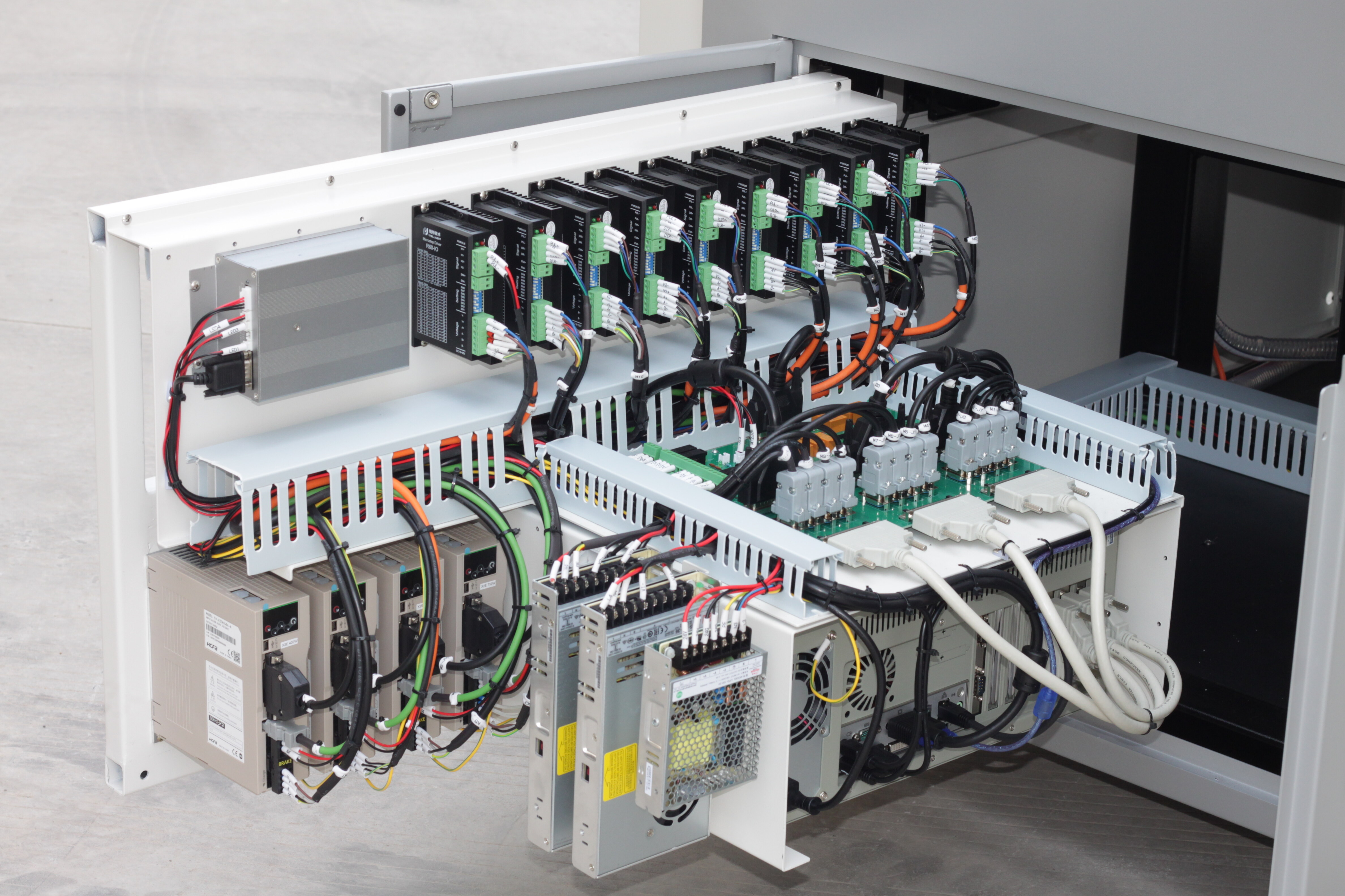
Solder Application: The solder wave or nozzle precisely targets the areas where soldering is required, typically through the use of computer-controlled motion systems. This ensures that solder is applied accurately and only where needed.
-
Cooling: After soldering, the PCB is cooled to solidify the solder joints and prevent component damage due to excessive heat.
-
Cleaning (optional): Depending on the application and requirements, the PCB may undergo a cleaning process to remove any flux residues left from the soldering process.
Selective wave soldering offers several advantages over traditional wave soldering:
-
Precision: It allows for precise and selective soldering of specific areas of the PCB, minimizing the risk of solder bridges or damage to sensitive components.
-
Cost-effectiveness: By soldering only the necessary areas, selective wave soldering can reduce material waste and minimize the need for manual touch-ups or rework.
-
Flexibility: It enables manufacturers to accommodate complex PCB designs with densely populated components or areas where hand soldering is impractical.
Description: Selective Wave Soldering is a specialized soldering process used in electronics manufacturing for soldering through-hole components onto printed circuit boards (PCBs). Unlike traditional wave soldering, which immerses entire PCBs in a molten solder wave, selective wave soldering targets specific areas of the PCB where through-hole components are located. This targeted approach allows for precise control over the soldering process, minimizing the risk of damaging sensitive components and improving overall soldering quality.
Key Features:
- Selective Soldering Nozzles: Utilizes selective soldering nozzles or jets to precisely apply solder to specific areas of the PCB where through-hole components are located.
- Programmable Soldering Patterns: Offers programmable soldering patterns and trajectories to accommodate various PCB designs and component layouts.
- High-Precision Control: Provides high-precision control over soldering parameters, including solder flow rate, temperature, and dwell time, ensuring consistent and reliable solder joints.
- Reduced Heat Exposure: Minimizes heat exposure to sensitive components and adjacent areas of the PCB, preventing thermal damage and ensuring component integrity.
- Efficient Flux Application: Applies flux selectively to the soldering areas to facilitate solder wetting and improve solder joint quality.
- Conveyor System: Integrates with conveyor systems to transport PCBs through the selective soldering process efficiently.
- Automated Operation: Supports automated operation with programmable controls and robotic integration, reducing manual labor and improving production efficiency.
Advantages:
- Improved Soldering Quality: Ensures high-quality solder joints with reduced defects and improved reliability.
- Enhanced Component Compatibility: Accommodates a wide range of through-hole components, including heat-sensitive or delicate parts.
- Cost Savings: Minimizes material waste and rework, resulting in cost savings and improved production yield.
- Flexible Production: Adaptable to various PCB designs and assembly requirements, offering flexibility in manufacturing processes.
- Reduced Environmental Impact: Optimizes solder usage and flux application, reducing environmental footprint and waste generation.
Applications:
- Electronics Assembly: Used in the assembly of PCBs for various electronic devices, including consumer electronics, automotive electronics, medical devices, aerospace components, and industrial equipment.
- Mixed Technology PCBs: Ideal for mixed technology PCBs containing both surface mount and through-hole components, providing a versatile soldering solution.
Selective Wave Soldering offers precise and efficient soldering of through-hole components on PCBs, ensuring high-quality solder joints while minimizing heat exposure and component damage. With its advanced features and benefits, this soldering process is widely used in electronics manufacturing for producing reliable and durable electronic assemblies.